Table of Contents
- Introduction to GLS Verification
- GLS in the ASIC Design Flow
- Why GLS is Critical
- GLS Fundamentals
- Setting Up GLS Environment
- GLS Testbench Considerations
- Timing Annotation and SDF
- Common GLS Issues and Debug
- GLS Best Practices
- Real-World Examples
- Advanced GLS Topics
- GLS Checklist
1. Introduction to GLS Verification
1.1 What is Gate-Level Simulation?
Gate-Level Simulation (GLS) is a verification technique that simulates the synthesized gate-level netlist of a design rather than the original RTL (Register Transfer Level) code. The netlist consists of standard cells from a technology library (AND gates, OR gates, flip-flops, etc.) connected together to implement the design functionality.
Key Characteristics:
- Operates on synthesized netlist (Verilog/VHDL netlist from synthesis tools)
- Uses technology library cell models
- Can include realistic gate delays and interconnect delays
- Verifies both functionality and timing
- Reuses RTL testbenches
1.2 GLS vs RTL Simulation
| Aspect | RTL Simulation | Gate-Level Simulation |
|---|---|---|
| Design Representation | High-level behavioral code | Netlist of standard cells |
| Abstraction Level | Register Transfer Level | Gate level (structural) |
| Speed | Fast (fewer events) | Slow (many gate transitions) |
| Timing | Idealized (zero delay or #1) | Realistic (actual gate/wire delays) |
| Models | RTL modules | Technology library cells |
| Purpose | Functional verification | Post-synthesis verification |
| X Propagation | Limited | Extensive (initialization issues) |
| Debug Ease | Easier (meaningful signal names) | Harder (synthesized names) |
1.3 Types of GLS
1.3.1 Zero-Delay GLS (Functional GLS)
- No timing information applied
- Verifies only functional correctness after synthesis
- Faster simulation
- Good for catching synthesis bugs
1.3.2 Unit-Delay GLS
- Each gate has fixed unit delay (e.g., #1)
- Simple timing check
- Helps identify some timing issues
1.3.3 Full-Timing GLS (with SDF)
- Uses SDF (Standard Delay Format) backannotation
- Contains actual gate and interconnect delays
- Most accurate timing verification
- Slower simulation
- Catches real timing violations
2. GLS in the ASIC Design Flow
2.1 GLS Position in Design Flow
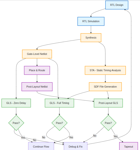
2.2 When to Run GLS
- Post-Synthesis GLS (Pre-Layout)
- After logic synthesis, before place-and-route
- Verifies synthesis correctness
- No parasitic extraction yet
- Uses estimated timing (SDF from synthesis)
- Post-Layout GLS
- After place-and-route
- Includes real parasitic extraction
- Most accurate timing
- Final verification before tapeout
- Iterative GLS
- During ECO (Engineering Change Order) cycles
- After design modifications
- Quick verification of changes
3. Why GLS is Critical
3.1 Problems Caught by GLS
3.1.1 Synthesis Tool Errors
Synthesis tools can occasionally misinterpret RTL intent or introduce bugs during optimization.
Example Issue:
// RTL Code
assign out = (a & b) | (c & d);

// Incorrectly synthesized to (rare, but possible):
// out = (a | b) & (c | d);
GLS will catch this functional mismatch.
3.1.2 X Propagation Issues
RTL simulation often masks initialization problems. GLS exposes uninitialized signals.
Example:
// RTL - flip-flop without reset
always @(posedge clk) begin
  data_out <= data_in;
end
- RTL Simulation: Initial value might default to 0
- GLS: Output starts as ‘X’ until first clock edge, propagates through logic
3.1.3 Timing Violations
Setup Time Violations:
Data arrives too late before clock edge
Hold Time Violations:
Data changes too soon after clock edge
Example Scenario:
- Long combinational path between two flip-flops
- RTL simulation: Assumes zero delay, works fine
- GLS with SDF: Data arrives after clock edge → setup violation → wrong data captured
3.1.4 Clock Domain Crossing (CDC) Issues
Metastability:
// No synchronizer - dangerous!
always @(posedge clk_fast) begin
  data_sync <= data_from_slow_domain; // Can catch metastable value
end
GLS with timing can expose CDC problems that RTL simulation misses.
3.1.5 Reset/Power-Up Sequence Issues
- Improper reset distribution
- Reset deassertion timing
- Power-up initialization
3.1.6 Glitches and Hazards
Combinational logic can produce glitches that RTL simulation doesn’t show but GLS captures.
Example:
// Combinational logic
assign out = (sel) ? a : b;

// During sel transition, 'out' might glitch if a≠b
3.2 Real-World GLS Failure Statistics
Based on industry experience:
| Issue Category | % of GLS Failures |
|---|---|
| X Propagation (uninitialized signals) | 35% |
| Timing Violations (setup/hold) | 25% |
| Clock Domain Crossing Issues | 15% |
| Reset Sequence Problems | 12% |
| Synthesis Mismatches | 8% |
| Other (glitches, race conditions) | 5% |
4. GLS Fundamentals
4.1 Gate-Level Netlist Structure
A synthesized netlist contains:
Example Netlist Fragment:
module counter_8bit (
  input wire clk,
  input wire rst_n,
  input wire enable,
  output wire [7:0] count
);

  wire n1, n2, n3, n4, n5;
  wire [7:0] count_reg;

  // Flip-flops from technology library
  DFFR_X1 count_reg_0_ (
    .D(n1),
    .CK(clk),
    .RN(rst_n),
    .Q(count_reg[0])
  );

  DFFR_X1 count_reg_1_ (
    .D(n2),
    .CK(clk),
    .RN(rst_n),
    .Q(count_reg[1])
  );

  // Combinational logic gates
  XOR2_X1 U10 (.A(count_reg[0]), .B(enable), .Z(n1));
  AND2_X1 U11 (.A1(count_reg[0]), .A2(enable), .Z(n3));
  XOR2_X1 U12 (.A(count_reg[1]), .B(n3), .Z(n2));

  // ... more gates ...

  assign count = count_reg;

endmodule
Key Elements:
DFFR_X1: D flip-flop with reset (from library)XOR2_X1,AND2_X1: Logic gates (from library)U10,U11,U12: Synthesizer-generated instance namesn1,n2,n3: Internal nets (auto-generated names)
4.2 Technology Libraries
Technology libraries provide cell models for simulation and timing.
Library Components:
- Functional Models (Liberty .lib format)
- Cell functionality (truth tables)
- Timing arcs (delays, setup/hold times)
- Power characteristics
- Simulation Models (Verilog)
- Behavioral models for each cell
- Can be fast (UDP-based) or detailed (switch-level)
Example Liberty Timing Arc:
cell (DFFR_X1) {
  pin(CK) {
    direction : input;
    capacitance : 0.005;
  }
  pin(D) {
    direction : input;
    timing() {
      related_pin : "CK";
      timing_type : setup_rising;
      rise_constraint(scalar) {
        values("0.15"); // 150ps setup time
      }
    }
  }
  pin(Q) {
    direction : output;
    timing() {
      related_pin : "CK";
      timing_sense : positive_unate;
      cell_rise(delay_template) {
        values("0.25"); // 250ps clock-to-Q delay
      }
    }
  }
}
4.3 SDF (Standard Delay Format)
SDF files contain timing information backannotated into the netlist.
Example SDF:
(DELAYFILE
  (SDFVERSION "3.0")
  (DESIGN "counter_8bit")
  (DATE "2024-01-15")
  (VENDOR "SynthesisTool")
  (PROGRAM "Synthesis")
  (VERSION "v2023.06")
  (DIVIDER /)
  (TIMESCALE 1ps)

  (CELL
    (CELLTYPE "DFFR_X1")
    (INSTANCE count_reg_0_)
    (DELAY
      (ABSOLUTE
        (IOPATH CK Q (250:280:310) (245:275:305))  // min:typ:max
        (IOPATH RN Q () (150:170:190))
      )
    )
    (TIMINGCHECK
      (SETUP D (posedge CK) (120:150:180))
      (HOLD D (posedge CK) (50:70:90))
    )
  )

  (CELL
    (CELLTYPE "XOR2_X1")
    (INSTANCE U10)
    (DELAY
      (ABSOLUTE
        (IOPATH A Z (80:100:120) (85:105:125))
        (IOPATH B Z (80:100:120) (85:105:125))
      )
    )
  )
)
SDF Annotation Modes:
- Minimum Timing: Best-case delays (fast corner)
- Typical Timing: Nominal delays
- Maximum Timing: Worst-case delays (slow corner)
5. Setting Up GLS Environment
5.1 Required Files
| File Type | Purpose | Example |
|---|---|---|
| Gate-level netlist | Synthesized design | design_netlist.v |
| Technology library models | Cell simulation models | tech_lib.v |
| Liberty file (.lib) | Timing/power data | tech_slow.lib |
| SDF file | Delay backannotation | design.sdf |
| Testbench | Stimulus and checking | tb_design.sv |
| Simulation script | Tool commands | run_gls.tcl |
5.2 Simulator Setup
5.2.1 VCS (Synopsys) Setup
Compilation Script (compile_gls.sh):
#!/bin/bash

# Set environment
export SYNOPSYS_HOME=/tools/synopsys/vcs
export VCS_HOME=$SYNOPSYS_HOME

# Define files
NETLIST="./netlist/design_netlist.v"
TECH_LIB="./libs/tech_lib.v"
TESTBENCH="./tb/tb_design.sv"
SDF_FILE="./sdf/design.sdf"

# Compile with VCS
vcs -sverilog \
    -full64 \
    -debug_access+all \
    -timescale=1ns/1ps \
    +v2k \
    -y ./libs +libext+.v \
    +define+SDF \
    +neg_tchk \
    +transport_int_delays \
    +pulse_int_e/0 \
    +pulse_int_r/0 \
    -sdf max:tb_design.dut:${SDF_FILE} \
    $TECH_LIB \
    $NETLIST \
    $TESTBENCH \
    -o simv_gls \
    -l compile_gls.log

# Key VCS options explained:
# -timescale=1ns/1ps : Set time precision
# +v2k : Verilog 2001 support
# +define+SDF : Define SDF macro for conditional code
# +neg_tchk : Enable negative timing check reporting
# +transport_int_delays : Use transport delays (more accurate)
# +pulse_int_e/0, +pulse_int_r/0 : Pulse width filtering (0 = no filter)
# -sdf max:instance:file : SDF backannotation
Run Script (run_gls.sh):
#!/bin/bash

# Run simulation
./simv_gls \
    +vcs+finish+100000000 \
    +ntb_random_seed=12345 \
    -l sim_gls.log \
    +vcd+design_gls.vcd

# Generate FSDB waveform (optional, better for debug)
./simv_gls \
    -ucli -i run.tcl \
    -l sim_gls.log
TCL Script for VCS (run.tcl):
# UCLI commands for VCS
run
dump -file design_gls.fsdb -type FSDB
dump -add tb_design -depth 0 -aggregates -scope .
run
quit
5.2.2 Xcelium (Cadence) Setup
Compilation and Run Script:
#!/bin/bash

# Set environment
export CADENCE_HOME=/tools/cadence/xcelium

NETLIST="./netlist/design_netlist.v"
TECH_LIB="./libs/tech_lib.v"
TESTBENCH="./tb/tb_design.sv"
SDF_FILE="./sdf/design.sdf"

# Compile and elaborate
xrun \
    -64bit \
    -sv \
    -timescale 1ns/1ps \
    -access +rwc \
    -sdf_cmd_file sdf.cmd \
    -input run_xcelium.tcl \
    -v $TECH_LIB \
    -v $NETLIST \
    $TESTBENCH \
    -l xrun_gls.log

# SDF command file (sdf.cmd):
# COMPILED_SDF_FILE = "design.sdf.X"
# INSTANCE = tb_design.dut
# TIMING = MAXIMUM
# LOG_FILE = sdf_annotate.log
SDF Command File (sdf.cmd):
# SDF annotation commands for Xcelium
COMPILED_SDF_FILE = "design.sdf.X",
    INSTANCE = tb_design.dut,
    TIMING = MAXIMUM,
    SCALE_FACTORS = "1.0:1.0:1.0",
    SCALE_TYPE = FROM_MAXIMUM,
    LOG_FILE = "sdf_annotate.log",
    MTM_CONTROL = "MAXIMUM",
    WARNING_COUNTER = 100
5.2.3 ModelSim/QuestaSim Setup
Compilation Script:
#!/bin/bash

# Create work library
vlib work
vmap work work

# Compile technology library
vlog -work work ./libs/tech_lib.v

# Compile netlist
vlog -work work ./netlist/design_netlist.v

# Compile testbench
vlog -sv -work work ./tb/tb_design.sv

# Run simulation with SDF
vsim -c -do "
    sdf load tb_design/dut ./sdf/design.sdf;
    run -all;
    quit
" tb_design -l sim_gls.log
5.3 Directory Structure Example
gls_verification/
├── netlist/
│   ├── design_netlist.v          # Post-synthesis netlist
│   └── design_netlist_mapped.v   # With pin mapping
├── libs/
│   ├── tech_lib.v                # Verilog library models
│   ├── tech_slow.lib             # Liberty slow corner
│   ├── tech_typical.lib          # Liberty typical corner
│   └── tech_fast.lib             # Liberty fast corner
├── sdf/
│   ├── design_slow.sdf           # Slow corner delays
│   ├── design_typical.sdf        # Typical delays
│   └── design_fast.sdf           # Fast corner delays
├── tb/
│   ├── tb_design.sv              # Main testbench
│   ├── test_vectors.txt          # Test data
│   └── expected_results.txt      # Golden reference
├── scripts/
│   ├── compile_gls.sh            # Compilation script
│   ├── run_gls.sh                # Run script
│   ├── run.tcl                   # Simulator TCL commands
│   └── sdf.cmd                   # SDF annotation commands
├── sim/
│   └── (simulation outputs)
└── results/
    ├── waveforms/
    └── logs/
6. GLS Testbench Considerations
6.1 Testbench Reuse from RTL
The same testbench used for RTL simulation can typically be reused for GLS with some modifications.
Key Considerations:
6.1.1 Timing Adjustments
RTL Testbench (Zero Delay):
// RTL testbench - works with zero delay
module tb_design;
  reg clk, rst_n;
  reg [7:0] data_in;
  wire [7:0] data_out;

  // Clock generation
  initial clk = 0;
  always #5 clk = ~clk; // 10ns period

  // Stimulus
  initial begin
    rst_n = 0;
    data_in = 8'h00;
    #20 rst_n = 1;
    #10 data_in = 8'hAA;
    #10 $display("Output: %h", data_out); // Checks immediately
  end

  // DUT instantiation
  design_rtl dut (
    .clk(clk),
    .rst_n(rst_n),
    .data_in(data_in),
    .data_out(data_out)
  );
endmodule
GLS Testbench (With Timing):
// GLS testbench - accounts for delays
module tb_design;
  reg clk, rst_n;
  reg [7:0] data_in;
  wire [7:0] data_out;

  // Clock generation - same
  initial clk = 0;
  always #5 clk = ~clk;

  // Stimulus - modified for GLS
  initial begin
    rst_n = 0;
    data_in = 8'h00;
    #20 rst_n = 1;
    #10 data_in = 8'hAA;
    #15 $display("Output: %h", data_out); // WAIT longer for delays
  end

  // DUT instantiation - change to netlist
  `ifdef GLS
    design_netlist dut (  // Gate-level netlist module
      .clk(clk),
      .rst_n(rst_n),
      .data_in(data_in),
      .data_out(data_out)
    );
  `else
    design_rtl dut (      // RTL module
      .clk(clk),
      .rst_n(rst_n),
      .data_in(data_in),
      .data_out(data_out)
    );
  `endif
endmodule
6.1.2 Handling X Propagation
GLS is more sensitive to uninitialized values. Add explicit initialization.
Example:
// BAD - May cause X propagation in GLS
reg [7:0] counter;
always @(posedge clk) begin
  counter <= counter + 1;  // counter starts as X!
end

// GOOD - Explicit initialization
reg [7:0] counter;
initial counter = 8'h00;  // Initialize to known value
always @(posedge clk or negedge rst_n) begin
  if (!rst_n)
    counter <= 8'h00;
  else
    counter <= counter + 1;
end
6.1.3 Setup and Hold Time Margins
Add margins to input changes relative to clock edges.
RTL – No margin needed:
always @(posedge clk) begin
  data_in <= new_value;  // Changes exactly at clock edge
end
GLS – Add margins:
// Change inputs in middle of clock phase (safe)
always @(posedge clk) begin
  #2 data_in <= new_value;  // 2ns after clock edge
end

// OR sample outputs well after clock edge
always @(posedge clk) begin
  #3 sampled_output = data_out;  // 3ns after clock
end
6.2 Clock Generation for GLS
6.2.1 Clock Skew Consideration
Single Clock Domain:
// Simple clock - OK for most cases
reg clk;
initial clk = 0;
always #5 clk = ~clk;  // 100MHz

// Apply to DUT
assign dut.clk = clk;
Multiple Clock Domains with Skew:
// Primary clock
reg clk_main;
initial clk_main = 0;
always #5 clk_main = ~clk_main;

// Derived clock with skew (realistic scenario)
reg clk_peripheral;
initial clk_peripheral = 0;
always #5.3 clk_peripheral = ~clk_peripheral;  // 300ps skew

// For GLS, might want to model clock tree delay
wire clk_to_dut;
assign #2 clk_to_dut = clk_main;  // 2ns clock tree delay
6.2.2 Clock Gating Verification
// RTL with clock gating
module design_with_cg (
  input clk,
  input enable,
  input [7:0] data_in,
  output reg [7:0] data_out
);
  // Synthesizer inserts ICG (Integrated Clock Gate)
  wire clk_gated;
  assign clk_gated = clk & enable;  // BAD - can glitch!

  always @(posedge clk_gated)
    data_out <= data_in;
endmodule
After synthesis:
// Netlist with proper ICG cell
module design_with_cg (
  input clk,
  input enable,
  input [7:0] data_in,
  output wire [7:0] data_out
);
  wire clk_gated;
  wire enable_latched;

  // Integrated Clock Gate cell from library
  ICG_X1 U_ICG (
    .CK(clk),
    .E(enable),
    .SE(1'b0),  // Scan enable
    .ECK(clk_gated)
  );

  // Flip-flops use gated clock
  DFFR_X1 data_out_reg_0_ (
    .D(data_in[0]),
    .CK(clk_gated),
    .RN(rst_n),
    .Q(data_out[0])
  );
  // ... more flip-flops
endmodule
GLS Testbench:
// Test clock gating behavior
initial begin
  clk = 0;
  enable = 0;
  data_in = 8'hAA;

  #100 enable = 1;  // Enable clock
  #20 data_in = 8'hBB;
  #20 enable = 0;   // Gate clock
  #20 data_in = 8'hCC;  // Should NOT be captured
  #20 enable = 1;   // Re-enable
  #20 data_in = 8'hDD;  // Should be captured

  #50 $finish;
end
6.3 Reset Strategy for GLS
6.3.1 Synchronous vs Asynchronous Reset
Synchronous Reset:
// RTL
always @(posedge clk) begin
  if (!rst_n)
    data <= 0;
  else
    data <= data_in;
end

// GLS consideration: Reset must be stable before first clock
initial begin
  rst_n = 0;
  #50;  // Hold reset for multiple clock cycles
  @(posedge clk);  // Wait for clock edge
  #2 rst_n = 1;    // Release after clock edge with margin
end
Asynchronous Reset:
// RTL
always @(posedge clk or negedge rst_n) begin
  if (!rst_n)
    data <= 0;
  else
    data <= data_in;
end

// GLS consideration: Reset deassertion recovery time
initial begin
  rst_n = 0;
  #50 rst_n = 1;  // Can deassert anytime, but...
  // Better: deassert synchronously to avoid recovery violations
  #50;
  @(posedge clk);
  #2 rst_n = 1;  // Safe deassertion
end
7. Timing Annotation and SDF
7.1 Understanding SDF Files
SDF (Standard Delay Format) is the industry-standard format for timing backannotation.
7.1.1 SDF File Structure
Complete SDF Example:
(DELAYFILE
  // Header information
  (SDFVERSION "3.0")
  (DESIGN "uart_transmitter")
  (DATE "2024-01-20 14:30:00")
  (VENDOR "SynthesisCorp")
  (PROGRAM "synthesis_tool")
  (VERSION "v2023.12")
  (DIVIDER /)              // Hierarchy separator
  (TIMESCALE 1ps)          // Time unit
  (VOLTAGE 1.08:1.2:1.32)  // Min:Typ:Max voltage
  (PROCESS "typical")
  (TEMPERATURE 25:27:125)  // Min:Typ:Max temperature

  // Timing for a flip-flop instance
  (CELL
    (CELLTYPE "DFFR_X1")
    (INSTANCE tx_state_reg_0_)
    (DELAY
      (ABSOLUTE
        // Clock-to-Q delay: (min:typ:max) for rise, fall
        (IOPATH (posedge CK) Q (180:250:320) (170:240:310))
        // Reset-to-Q delay
        (IOPATH (negedge RN) Q () (120:150:180))
      )
    )
    (TIMINGCHECK
      // Setup time for data relative to clock
      (SETUP D (posedge CK) (100:120:150))
      (SETUP (negedge D) (posedge CK) (95:115:145))
      // Hold time for data relative to clock
      (HOLD D (posedge CK) (40:50:65))
      (HOLD (negedge D) (posedge CK) (35:45:60))
      // Minimum pulse width
      (WIDTH (posedge CK) (200:250:300))
      (WIDTH (negedge CK) (200:250:300))
      // Recovery time after reset
      (RECOVERY (posedge RN) (posedge CK) (150:180:220))
      // Removal time for reset
      (REMOVAL (posedge RN) (posedge CK) (50:70:90))
    )
  )

  // Timing for a combinational gate
  (CELL
    (CELLTYPE "AND2_X1")
    (INSTANCE U_AND_123)
    (DELAY
      (ABSOLUTE
        // Input A to output Z: rise and fall delays
        (IOPATH A Z (60:80:105) (55:75:100))
        // Input B to output Z
        (IOPATH B Z (65:85:110) (60:80:105))
      )
    )
  )

  // Timing for interconnect (wire delays)
  (CELL
    (CELLTYPE "INTERCONNECT")
    (INSTANCE)
    (DELAY
      (ABSOLUTE
        // Net delay from driver pin to load pin
        (INTERCONNECT U_AND_123/Z U_OR_456/A (25:35:50))
        (INTERCONNECT U_AND_123/Z tx_state_reg_1_/D (30:40:55))
      )
    )
  )
)
7.1.2 SDF Timing Checks
Setup and Hold Timing Checks:
(SETUP data_signal (posedge clock_signal) (setup_time))
(HOLD data_signal (posedge clock_signal) (hold_time))

// Example
(SETUP D (posedge CK) (100:120:150))
(HOLD D (posedge CK) (40:50:65))
7.2 SDF Backannotation Process
7.2.1 Annotation Modes
Maximum Timing (Slow Corner):
# VCS syntax
-sdf max:instance_path:slow_corner.sdf

# Use for: Setup time verification, worst-case delay
Minimum Timing (Fast Corner):
-sdf min:instance_path:fast_corner.sdf

# Use for: Hold time verification, best-case delay
7.2.2 Handling Timing Violations
Setup Time Violations:
- Data arrives too late before clock edge
- Simulator drives output to X
- Warning issued in log
Hold Time Violations:
- Data changes too soon after clock edge
- May capture wrong data
- Output becomes X
8. Common GLS Issues and Debug
8.1 X Propagation Issues
8.1.1 Uninitialized Registers
Problem: Registers without reset propagate X values in GLS.
Example:
// RTL - No reset on this register
always @(posedge clk) begin
  temp_reg <= input_data;  // Starts as X in GLS!
end
Symptoms:
Warning: Signal temp_reg has value 'X' at time 100ns
Error: Assertion failed - output_valid is 'X', expected 1'b1
Debug Steps:
- Find the X source in waveform
- Trace back through netlist
- Identify uninitialized flip-flop
Solution:
// Add reset
always @(posedge clk or negedge rst_n) begin
  if (!rst_n)
    temp_reg <= 8'h00;  // Initialize to known value
  else
    temp_reg <= input_data;
end
8.1.2 Combinational Loops
Problem: Feedback loops without registers cause X propagation.
RTL Example:
// Problematic code
assign out = sel ? in : out;  // Combinational feedback!
Netlist Result:
Warning: Combinational loop detected involving net 'out'
Signal 'out' stuck at X
Solution: Break loop with a register:
always @(posedge clk) begin
  out <= sel ? in : out;  // Now sequential
end
8.1.3 Array Index Out of Bounds
Problem: X from invalid memory access.
Example:
reg [7:0] mem [0:15];  // 16 entries
reg [4:0] index;       // Can address up to 31!

assign data_out = mem[index];  // May access out of bounds
GLS Behavior:
When index > 15: data_out = 8'hXX
Solution:
// Clamp index
wire [3:0] safe_index;
assign safe_index = (index > 15) ? 4'd15 : index[3:0];
assign data_out = mem[safe_index];
8.2 Clock Domain Crossing (CDC) Issues
8.2.1 Missing Synchronizers
Problem: Data crosses clock domains without synchronization.
Bad Code:
// Clock domain A
always @(posedge clk_a) begin
  data_a <= input_data;
end

// Clock domain B - WRONG!
always @(posedge clk_b) begin
  data_b <= data_a;  // Direct connection, no sync!
end
GLS Symptoms:
- Metastability (signal oscillates between 0 and 1)
- Random X values
- Incorrect data capture
Waveform Example of Metastability:
clk_b:   _____/‾‾‾‾\____/‾‾‾‾\____
data_a:  ______/‾‾‾‾‾‾‾‾‾\_________  (from clk_a domain)
data_b:  ______XXXX‾‾‾‾‾\__________  (X = metastable!)
Solution – Two-Stage Synchronizer:
// Proper CDC synchronizer
reg data_sync1, data_sync2;

always @(posedge clk_b or negedge rst_n) begin
  if (!rst_n) begin
    data_sync1 <= 1'b0;
    data_sync2 <= 1'b0;
  end else begin
    data_sync1 <= data_a;      // First stage
    data_sync2 <= data_sync1;  // Second stage
  end
end

assign data_b = data_sync2;  // Use synchronized data
8.2.2 Gray Code for Multi-Bit CDC
Problem: Multi-bit values crossing domains can be corrupted.
Example – FIFO Pointers:
// Write domain
reg [3:0] wr_ptr_bin;  // Binary counter
always @(posedge wr_clk) begin
  wr_ptr_bin <= wr_ptr_bin + 1;
end

// BAD: Synchronize binary directly to read domain
// When wr_ptr changes from 0111 (7) to 1000 (8),
// read domain might see intermediate values like 1111!
Solution – Gray Code:
// Convert to Gray before crossing
wire [3:0] wr_ptr_gray;
assign wr_ptr_gray = wr_ptr_bin ^ (wr_ptr_bin >> 1);

// Synchronize Gray code
reg [3:0] wr_ptr_gray_sync1, wr_ptr_gray_sync2;
always @(posedge rd_clk) begin
  wr_ptr_gray_sync1 <= wr_ptr_gray;
  wr_ptr_gray_sync2 <= wr_ptr_gray_sync1;
end

// Convert back to binary in read domain
reg [3:0] wr_ptr_bin_sync;
assign wr_ptr_bin_sync[3] = wr_ptr_gray_sync2[3];
assign wr_ptr_bin_sync[2] = wr_ptr_bin_sync[3] ^ wr_ptr_gray_sync2[2];
assign wr_ptr_bin_sync[1] = wr_ptr_bin_sync[2] ^ wr_ptr_gray_sync2[1];
assign wr_ptr_bin_sync[0] = wr_ptr_bin_sync[1] ^ wr_ptr_gray_sync2[0];
8.3 Reset Issues
8.3.1 Incomplete Reset Coverage
Problem: Some registers lack reset, causing X after GLS reset.
Debug Approach:
# Search for X values after reset in simulation log
grep "time.*after reset.*X" sim_gls.log

# In waveform: Add all registers, look for X's after reset release
Systematic Check:
// Add assertion to catch unreset registers
property no_x_after_reset;
  @(posedge clk) disable iff (!rst_n)
  $stable(rst_n) && rst_n |-> !$isunknown(critical_signal);
endproperty
assert property (no_x_after_reset);
8.3.2 Reset Tree Skew
Problem: Reset reaches different parts of design at different times.
Scenario:
Module A reset at t=100ns
Module B reset at t=102ns (due to buffer delays)

If A sends data to B immediately after reset:
- A thinks B is ready
- B still in reset, drops data
Solution:
// Wait for reset to propagate everywhere
initial begin
  rst_n = 0;
  #100 rst_n = 1;

  // Wait extra time for reset to reach all logic
  #50;

  // Now start test
  start_test_sequence();
end
8.4 Simulation Speed Issues
8.4.1 Why GLS is Slow
| Factor | Impact | Typical Slowdown |
|---|---|---|
| Gate count | 10K-1M gates vs few RTL modules | 10-100x |
| Event density | Every gate transition = event | 50-200x |
| Timing annotation | SDF delay calculations | 2-5x additional |
| X propagation | More unknowns to track | 1.5-3x |
| Total | Combined effect | 100-1000x slower than RTL |
Example:
RTL simulation: 1 million cycles in 10 seconds
GLS simulation: 1 million cycles in 2-3 hours
8.4.2 Speed Optimization Techniques
1. Use Compiled Simulation
# VCS - compile to binary
vcs +vcs+lic+wait -full64 netlist.v tb.sv -o simv
./simv

# vs interpreted mode (much slower)
vcs -R netlist.v tb.sv
2. Reduce Waveform Dumping
// Don't dump everything
initial begin
  $dumpfile("design.vcd");
  // Only dump specific modules
  $dumpvars(0, tb.dut.critical_path);
  $dumpvars(0, tb.dut.debug_signals);
  // NOT: $dumpvars(0, tb.dut);  // Too much data!
end
3. Use Fast Library Models
// Technology library often provides multiple models:
// - Detailed: Switch-level, very accurate, slow
// - UDP: User-Defined Primitives, faster
// - Behavioral: Fastest, less accurate

// Use UDP or behavioral models for GLS
4. Selective SDF Annotation
# Annotate only critical paths
-sdf max:tb.dut.critical_module:critical.sdf

# Don't annotate non-timing-critical blocks
# (they run faster without SDF)
5. Run Shorter Tests
// Break long tests into smaller chunks
// Run quick tests in GLS, extensive tests in RTL

// Example: Instead of 1M cycle test:
// - RTL: 1M cycles (full coverage)
// - GLS: 10K cycles (focused on timing-critical scenarios)
8.5 Debug Methodology
8.5.1 Comparison with RTL
Golden Reference Approach:
// Dual simulation: RTL and GLS
module tb_compare;
  // Instantiate RTL
  design_rtl dut_rtl (
    .clk(clk),
    .rst_n(rst_n),
    .in(data_in),
    .out(out_rtl)
  );

  // Instantiate GLS netlist
  design_netlist dut_gls (
    .clk(clk),
    .rst_n(rst_n),
    .in(data_in),
    .out(out_gls)
  );

  // Compare outputs
  always @(posedge clk) begin
    if (rst_n) begin
      if (out_rtl !== out_gls) begin
        $error("Mismatch at time %t: RTL=%h, GLS=%h",
               $time, out_rtl, out_gls);
      end
    end
  end
endmodule
8.5.2 Hierarchical Debug
Step-by-step narrowing:
1. Find failing test
2. Identify failing cycle
3. Find failing output signal
4. Trace signal back to source
5. Find first point of divergence from RTL
6. Analyze gates around that point
Example Debug Session:
// 1. Failure detected
$error("Output mismatch at time 1234ns");

// 2. Add probes around failure time
$monitor("Time=%t clk=%b data=%h", $time, clk, critical_data);

// 3. Trace critical_data backwards in netlist
// In waveform viewer:
// - Select critical_data signal
// - "Find drivers" or "Trace fanin"
// - Walk back through gates until finding X or mismatch

// 4. Common findings:
// - Uninitialized register
// - Timing violation
// - Missing/wrong gate in netlist
8.5.3 Using Simulator Debug Features
VCS Debug:
# Compile with debug symbols
vcs -debug_access+all netlist.v tb.sv

# Run with GUI
./simv -gui

# In GUI:
# - Set breakpoints on $error
# - Step through waveform
# - Cross-probe netlist to waveform
Useful VCS Commands:
# In DVE (Discovery Visualization Environment)
scope tb.dut                    # Navigate hierarchy
add wave *                      # Add all signals
add wave -r tb.dut.submodule/*  # Add recursively
run 1000ns                      # Run simulation
bp $error                       # Break on error
9. GLS Best Practices
9.1 Pre-GLS Preparation Checklist
| Task | Purpose | Status |
|---|---|---|
| RTL simulations pass 100% | Ensure RTL is functionally correct | ☐ |
| Synthesis completed without errors | Clean synthesis required for GLS | ☐ |
| Netlist generated and reviewed | Verify netlist exists and loads | ☐ |
| Library models available | Ensure all cells have simulation models | ☐ |
| SDF file generated (if doing timing) | Timing annotation source | ☐ |
| Testbench reviewed for GLS compatibility | Check for timing-sensitive code | ☐ |
| Reset strategy verified | All registers have proper reset | ☐ |
| Clock generation reviewed | Clean clocks without glitches | ☐ |
9.2 GLS Strategy
9.2.1 Phased Approach
Phase 1: Zero-Delay GLS (Functional Only)
Goal: Catch synthesis errors and X propagation
Duration: First pass, relatively fast
What to check:
- Functionality matches RTL
- No X propagation issues
- All resets working properly
Phase 2: Unit-Delay GLS
Goal: Quick timing sanity check
Duration: Slightly slower than zero-delay
What to check:
- Basic timing relationships
- No gross timing violations
Phase 3: Full-Timing GLS (SDF Max/Slow Corner)
Goal: Setup time verification
Duration: Slowest
What to check:
- Setup violations
- Worst-case timing paths
- Maximum frequency operation
Phase 4: Full-Timing GLS (SDF Min/Fast Corner)
Goal: Hold time verification
Duration: Slowest
What to check:
- Hold violations
- Best-case timing paths
- Clock domain crossing issues
9.2.2 Regression Strategy
GLS Test Suite (Subset of RTL Tests):
RTL Regression: 1000 tests, 8 hours
GLS Regression: 50 tests (5% of RTL), 8 hours

Selection criteria for GLS tests:
1. Critical functionality tests
2. Corner case tests
3. Known timing-sensitive scenarios
4. Clock domain crossing tests
5. Reset sequence tests
Test Selection Example:
# gls_test_select.py
gls_tests = [
    "test_basic_functionality",      # Sanity
    "test_max_throughput",            # Performance critical
    "test_clock_domain_crossing",     # CDC sensitive
    "test_reset_sequence",            # Initialization
    "test_back_to_back_transfers",    # Timing critical
    "test_corner_case_overflow",      # Edge case
]
9.3 Coverage Goals for GLS
You can’t achieve same coverage as RTL due to time constraints. Focus on:
Functional Coverage (Target: 80-90% of RTL coverage)
- All major features exercised
- Critical corner cases hit
Code Coverage (Target: Not primary goal for GLS)
- GLS is about timing, not new functional coverage
- Use RTL simulation for code coverage
Toggle Coverage (Target: 50-70% of RTL)
- Verify major signals toggle
- Catch stuck-at faults
9.4 Synthesis Quality Checks
Before running GLS, verify synthesis quality:
Timing Reports:
# Check STA reports from synthesis
cat synthesis_timing_report.txt | grep "slack"

# Look for:
# - Positive slack on all paths (or minimal violations)
# - No huge negative slack
# - Reasonable clock frequency achieved
Area Reports:
# Check for unusual gate counts
cat synthesis_area_report.txt

# Red flags:
# - Excessive buffer/inverter count (routing congestion)
# - Very large combinational modules (long paths)
Synthesis Warnings:
# Review synthesis log carefully
grep -i "warning" synthesis.log

# Common issues to check:
# - Latches inferred (usually unintended)
# - Black boxes (missing modules)
# - Timing not met
# - Multi-driven nets
9.5 Sign-off Criteria
GLS considered passing when:
- ✅ All functional tests pass (same results as RTL)
- ✅ No X propagation issues (except explicitly expected cases)
- ✅ No setup violations (at target frequency with margins)
- ✅ No hold violations (at all frequency corners)
- ✅ No unexpected warnings in simulation log
- ✅ SDF annotation completed 100% successfully
- ✅ All assertions pass (same as RTL simulation)
- ✅ Coverage goals met (per defined targets)
Example Sign-off Report:
=== GLS Verification Sign-off Report ===
Design: UART_Controller
Date: 2024-01-20

Test Results:
  Total tests run: 50
  Tests passed: 50
  Tests failed: 0
  Pass rate: 100%

Timing Verification:
  Setup violations: 0
  Hold violations: 0
  Recovery violations: 0
  Removal violations: 0

SDF Annotation:
  Cells annotated: 2543/2543 (100%)
  Nets annotated: 1872/1872 (100%)
  Warnings: 0
  Errors: 0

X Propagation:
  Unexpected X's: 0
  Known X's (expected): 3 (reset scenarios)

Status: ✅ PASSED - Ready for tapeout
10. Real-World Examples
10.1 Example 1: UART Transmitter GLS
10.1.1 Design Overview
Specifications:
- 8-bit data transmission
- Configurable baud rate
- Standard 8N1 format (8 data bits, no parity, 1 stop bit)
- 100MHz system clock
- Target baud rate: 115200 bps
RTL Module:
module uart_tx (
  input wire clk,           // 100MHz system clock
  input wire rst_n,         // Active-low reset
  input wire [7:0] data_in, // Data to transmit
  input wire valid,         // Data valid strobe
  output reg ready,         // Ready for new data
  output reg tx_out         // Serial output
);

  // Baud rate generator
  parameter BAUD_DIV = 868;  // 100MHz / 115200 ≈ 868

  reg [9:0] baud_counter;
  reg baud_tick;

  // FSM states
  typedef enum reg [2:0] {
    IDLE  = 3'b000,
    START = 3'b001,
    DATA  = 3'b010,
    STOP  = 3'b011
  } state_t;

  state_t state, next_state;
  reg [2:0] bit_count;
  reg [7:0] shift_reg;

  // Baud rate generator
  always @(posedge clk or negedge rst_n) begin
    if (!rst_n) begin
      baud_counter <= 0;
      baud_tick <= 0;
    end else begin
      if (baud_counter == BAUD_DIV-1) begin
        baud_counter <= 0;
        baud_tick <= 1;
      end else begin
        baud_counter <= baud_counter + 1;
        baud_tick <= 0;
      end
    end
  end

  // FSM and datapath
  always @(posedge clk or negedge rst_n) begin
    if (!rst_n) begin
      state <= IDLE;
      bit_count <= 0;
      shift_reg <= 0;
      tx_out <= 1;
      ready <= 1;
    end else begin
      state <= next_state;

      case (state)
        IDLE: begin
          ready <= 1;
          tx_out <= 1;
          if (valid && ready) begin
            shift_reg <= data_in;
            ready <= 0;
          end
        end

        START: begin
          if (baud_tick) begin
            tx_out <= 0;  // Start bit
          end
        end

        DATA: begin
          if (baud_tick) begin
            tx_out <= shift_reg[0];
            shift_reg <= shift_reg >> 1;
            bit_count <= bit_count + 1;
          end
        end

        STOP: begin
          if (baud_tick) begin
            tx_out <= 1;  // Stop bit
          end
        end
      endcase
    end
  end

  // FSM next state logic
  always @(*) begin
    next_state = state;
    case (state)
      IDLE:  if (valid && ready) next_state = START;
      START: if (baud_tick) next_state = DATA;
      DATA:  if (baud_tick && bit_count == 7) next_state = STOP;
      STOP:  if (baud_tick) next_state = IDLE;
    endcase
  end

endmodule
10.1.2 GLS Setup
Files Required:
uart_tx_gls/
├── rtl/
│   └── uart_tx.sv
├── netlist/
│   └── uart_tx_netlist.v
├── libs/
│   ├── tech_lib.v
│   └── tech_lib_slow.lib
├── sdf/
│   ├── uart_tx_slow.sdf
│   └── uart_tx_fast.sdf
├── tb/
│   └── tb_uart_tx.sv
└── scripts/
    └── run_gls.sh
Testbench (tb_uart_tx.sv):
module tb_uart_tx;
  reg clk, rst_n;
  reg [7:0] data_in;
  reg valid;
  wire ready;
  wire tx_out;

  // Clock generation - 100MHz
  initial clk = 0;
  always #5 clk = ~clk;  // 10ns period

  // DUT instantiation
  `ifdef GLS
    uart_tx_netlist dut (
      .clk(clk),
      .rst_n(rst_n),
      .data_in(data_in),
      .valid(valid),
      .ready(ready),
      .tx_out(tx_out)
    );
  `else
    uart_tx dut (
      .clk(clk),
      .rst_n(rst_n),
      .data_in(data_in),
      .valid(valid),
      .ready(ready),
      .tx_out(tx_out)
    );
  `endif

  // Test sequence
  initial begin
    // Initialize
    rst_n = 0;
    data_in = 0;
    valid = 0;

    // Reset sequence (GLS-safe)
    repeat(10) @(posedge clk);
    #2 rst_n = 1;  // Deassert with margin after clock

    // Wait for reset to propagate
    repeat(5) @(posedge clk);

    // Test 1: Send byte 0xA5
    @(posedge clk);
    #2 begin  // Margin after clock
      data_in = 8'hA5;
      valid = 1;
    end

    @(posedge clk);
    #2 valid = 0;

    // Wait for transmission (10 bits * 868 clocks ≈ 8680 clocks)
    repeat(9000) @(posedge clk);

    // Test 2: Back-to-back bytes
    wait(ready);
    @(posedge clk);
    #2 begin
      data_in = 8'h5A;
      valid = 1;
    end
    @(posedge clk);
    #2 valid = 0;

    repeat(9000) @(posedge clk);

    $display("Test completed");
    $finish;
  end

  // Monitor
  initial begin
    $monitor("Time=%t rst_n=%b valid=%b ready=%b tx_out=%b data=%h",
             $time, rst_n, valid, ready, tx_out, data_in);
  end

  // Waveform dump
  initial begin
    `ifdef GLS
      $dumpfile("uart_tx_gls.vcd");
    `else
      $dumpfile("uart_tx_rtl.vcd");
    `endif
    $dumpvars(0, tb_uart_tx);
  end
endmodule
10.1.3 GLS Run Script
run_gls.sh:
#!/bin/bash

echo "=== UART TX GLS Verification ==="

# Step 1: Compile
echo "Step 1: Compiling design..."
vcs -sverilog \
    -full64 \
    -debug_access+all \
    -timescale=1ns/1ps \
    +define+GLS \
    +define+SDF \
    -sdf max:tb_uart_tx.dut:./sdf/uart_tx_slow.sdf \
    ./libs/tech_lib.v \
    ./netlist/uart_tx_netlist.v \
    ./tb/tb_uart_tx.sv \
    -o simv_uart_gls \
    -l compile_gls.log

if [ $? -eq 0 ]; then
    echo "✓ Compilation successful"
else
    echo "✗ Compilation failed - check compile_gls.log"
    exit 1
fi

# Step 2: Run simulation
echo "Step 2: Running GLS..."
./simv_uart_gls -l sim_gls.log

# Step 3: Check results
echo "Step 3: Checking results..."
if grep -q "Test completed" sim_gls.log; then
    echo "✓ Test completed"
else
    echo "✗ Test did not complete"
fi

if grep -qi "error" sim_gls.log; then
    echo "✗ Errors found in simulation"
    grep -i "error" sim_gls.log
    exit 1
else
    echo "✓ No errors"
fi

if grep -qi "violation" sim_gls.log; then
    echo "✗ Timing violations found"
    grep -i "violation" sim_gls.log
    exit 1
else
    echo "✓ No timing violations"
fi

echo "=== GLS PASSED ==="
10.1.4 Common Issues Found
Issue 1: X Propagation in shift_reg
Problem:
Warning: Signal shift_reg has unknown value 'X' at time 100ns
Root Cause:
The shift register wasn’t fully initialized in reset.
Fix:
// Before (incomplete reset)
if (!rst_n) begin
  state <= IDLE;
  // shift_reg not reset!
end

// After (complete reset)
if (!rst_n) begin
  state <= IDLE;
  shift_reg <= 8'h00;  // Initialize shift register
end
Issue 2: Setup Violation on baud_counter
Problem:
$setuphold violation: data signal 'baud_counter[9]' changed at 999.8ns
                      clock edge 'clk' at 1000.0ns
                      Required setup time: 150ps, Actual: 50ps
Root Cause:
Long combinational path in baud counter increment logic.
Analysis:
Path: baud_counter[0] -> adder chain -> baud_counter[9] -> DFF
Delay: Clock-to-Q (250ps) + 9-bit adder (1800ps) + routing (200ps) = 2250ps
Setup time: 150ps
Total: 2400ps

Clock period: 10ns (100MHz) - Should be OK!

But SDF shows actual delays are longer in slow corner:
Clock-to-Q: 350ps
Adder: 2500ps
Routing: 300ps
Setup: 180ps
Total: 3330ps >> 10ns period is violated!
Solution: Requires RTL fix or slower clock. This is a design issue, not a test issue.
10.2 Example 2: Async FIFO with Clock Domain Crossing
10.2.1 Design Overview
Specifications:
- Asynchronous FIFO (different read/write clock domains)
- Depth: 16 entries
- Data width: 8 bits
- Gray code pointer synchronization
- Full and empty flags
Key GLS Challenges:
- Clock domain crossing verification
- Metastability detection
- Gray code synchronizer timing
- Full/empty flag generation timing
RTL Module (Simplified):
module async_fifo #(
  parameter DATA_WIDTH = 8,
  parameter DEPTH = 16,
  parameter ADDR_WIDTH = 4
)(
  // Write port
  input  wire                  wr_clk,
  input  wire                  wr_rst_n,
  input  wire [DATA_WIDTH-1:0] wr_data,
  input  wire                  wr_en,
  output wire                  wr_full,

  // Read port
  input  wire                  rd_clk,
  input  wire                  rd_rst_n,
  output wire [DATA_WIDTH-1:0] rd_data,
  input  wire                  rd_en,
  output wire                  rd_empty
);

  // Memory array
  reg [DATA_WIDTH-1:0] mem [0:DEPTH-1];

  // Write domain pointers
  reg [ADDR_WIDTH:0] wr_ptr_bin;
  reg [ADDR_WIDTH:0] wr_ptr_gray;

  // Read domain pointers
  reg [ADDR_WIDTH:0] rd_ptr_bin;
  reg [ADDR_WIDTH:0] rd_ptr_gray;

  // Synchronized pointers
  reg [ADDR_WIDTH:0] wr_ptr_gray_sync1, wr_ptr_gray_sync2;
  reg [ADDR_WIDTH:0] rd_ptr_gray_sync1, rd_ptr_gray_sync2;

  // Write domain logic
  always @(posedge wr_clk or negedge wr_rst_n) begin
    if (!wr_rst_n) begin
      wr_ptr_bin <= 0;
      wr_ptr_gray <= 0;
    end else if (wr_en && !wr_full) begin
      mem[wr_ptr_bin[ADDR_WIDTH-1:0]] <= wr_data;
      wr_ptr_bin <= wr_ptr_bin + 1;
      wr_ptr_gray <= (wr_ptr_bin + 1) ^ ((wr_ptr_bin + 1) >> 1);
    end
  end

  // Synchronize read pointer to write domain
  always @(posedge wr_clk or negedge wr_rst_n) begin
    if (!wr_rst_n) begin
      rd_ptr_gray_sync1 <= 0;
      rd_ptr_gray_sync2 <= 0;
    end else begin
      rd_ptr_gray_sync1 <= rd_ptr_gray;
      rd_ptr_gray_sync2 <= rd_ptr_gray_sync1;
    end
  end

  // Convert synced read pointer to binary for full calculation
  wire [ADDR_WIDTH:0] rd_ptr_bin_sync;
  assign rd_ptr_bin_sync[ADDR_WIDTH] = rd_ptr_gray_sync2[ADDR_WIDTH];
  genvar i;
  generate
    for (i = ADDR_WIDTH-1; i >= 0; i = i - 1) begin : gray_to_bin_wr
      assign rd_ptr_bin_sync[i] = rd_ptr_bin_sync[i+1] ^ rd_ptr_gray_sync2[i];
    end
  endgenerate

  // Full flag generation
  assign wr_full = (wr_ptr_bin[ADDR_WIDTH] != rd_ptr_bin_sync[ADDR_WIDTH]) &&
                   (wr_ptr_bin[ADDR_WIDTH-1:0] == rd_ptr_bin_sync[ADDR_WIDTH-1:0]);

  // Read domain logic
  always @(posedge rd_clk or negedge rd_rst_n) begin
    if (!rd_rst_n) begin
      rd_ptr_bin <= 0;
      rd_ptr_gray <= 0;
    end else if (rd_en && !rd_empty) begin
      rd_ptr_bin <= rd_ptr_bin + 1;
      rd_ptr_gray <= (rd_ptr_bin + 1) ^ ((rd_ptr_bin + 1) >> 1);
    end
  end

  // Synchronize write pointer to read domain
  always @(posedge rd_clk or negedge rd_rst_n) begin
    if (!rd_rst_n) begin
      wr_ptr_gray_sync1 <= 0;
      wr_ptr_gray_sync2 <= 0;
    end else begin
      wr_ptr_gray_sync1 <= wr_ptr_gray;
      wr_ptr_gray_sync2 <= wr_ptr_gray_sync1;
    end
  end

  // Convert synced write pointer to binary for empty calculation
  wire [ADDR_WIDTH:0] wr_ptr_bin_sync;
  assign wr_ptr_bin_sync[ADDR_WIDTH] = wr_ptr_gray_sync2[ADDR_WIDTH];
  generate
    for (i = ADDR_WIDTH-1; i >= 0; i = i - 1) begin : gray_to_bin_rd
      assign wr_ptr_bin_sync[i] = wr_ptr_bin_sync[i+1] ^ wr_ptr_gray_sync2[i];
    end
  endgenerate

  // Empty flag generation
  assign rd_empty = (rd_ptr_bin == wr_ptr_bin_sync);

  // Read data output
  assign rd_data = mem[rd_ptr_bin[ADDR_WIDTH-1:0]];

endmodule
10.2.2 GLS-Specific Testbench
tb_async_fifo_gls.sv:
module tb_async_fifo_gls;

  // Write clock domain - 100MHz
  reg wr_clk, wr_rst_n;
  reg [7:0] wr_data;
  reg wr_en;
  wire wr_full;

  // Read clock domain - 80MHz (different frequency!)
  reg rd_clk, rd_rst_n;
  wire [7:0] rd_data;
  reg rd_en;
  wire rd_empty;

  // Clock generation
  initial wr_clk = 0;
  always #5 wr_clk = ~wr_clk;  // 100MHz (10ns period)

  initial rd_clk = 0;
  always #6.25 rd_clk = ~rd_clk;  // 80MHz (12.5ns period)

  // DUT instantiation
  `ifdef GLS
    async_fifo_netlist dut (
      .wr_clk(wr_clk),
      .wr_rst_n(wr_rst_n),
      .wr_data(wr_data),
      .wr_en(wr_en),
      .wr_full(wr_full),
      .rd_clk(rd_clk),
      .rd_rst_n(rd_rst_n),
      .rd_data(rd_data),
      .rd_en(rd_en),
      .rd_empty(rd_empty)
    );
  `else
    async_fifo dut (
      .wr_clk(wr_clk),
      .wr_rst_n(wr_rst_n),
      .wr_data(wr_data),
      .wr_en(wr_en),
      .wr_full(wr_full),
      .rd_clk(rd_clk),
      .rd_rst_n(rd_rst_n),
      .rd_data(rd_data),
      .rd_en(rd_en),
      .rd_empty(rd_empty)
    );
  `endif

  // Scoreboard for checking
  reg [7:0] expected_data [$];

  // Write process
  initial begin
    wr_rst_n = 0;
    wr_data = 0;
    wr_en = 0;

    // Reset with proper timing
    repeat(20) @(posedge wr_clk);
    @(posedge wr_clk) #2 wr_rst_n = 1;

    // Wait for synchronizers to settle
    repeat(10) @(posedge wr_clk);

    // Write 20 bytes
    repeat(20) begin
      @(posedge wr_clk);
      if (!wr_full) begin
        #2 begin  // Margin after clock
          wr_data = $random;
          wr_en = 1;
          expected_data.push_back(wr_data);
          $display("[WR] Time=%t Writing data=%h", $time, wr_data);
        end
      end else begin
        $display("[WR] Time=%t FIFO FULL, waiting...", $time);
        wr_en = 0;
      end
    end

    @(posedge wr_clk) #2 wr_en = 0;
  end

  // Read process
  initial begin
    rd_rst_n = 0;
    rd_en = 0;

    // Reset with proper timing
    repeat(20) @(posedge rd_clk);
    @(posedge rd_clk) #2 rd_rst_n = 1;

    // Wait for synchronizers and some writes
    repeat(30) @(posedge rd_clk);

    // Read data and check
    repeat(25) begin
      @(posedge rd_clk);
      if (!rd_empty) begin
        #2 rd_en = 1;
        @(posedge rd_clk);
        #3;  // Wait for data to be available after clock

        if (expected_data.size() > 0) begin
          automatic reg [7:0] exp = expected_data.pop_front();
          if (rd_data === exp) begin
            $display("[RD] Time=%t Read data=%h OK", $time, rd_data);
          end else begin
            $error("[RD] Time=%t Data mismatch! Expected=%h, Got=%h",
                   $time, exp, rd_data);
          end
        end
      end else begin
        $display("[RD] Time=%t FIFO EMPTY", $time);
        rd_en = 0;
      end
    end

    // Check that we read everything
    if (expected_data.size() == 0) begin
      $display("*** TEST PASSED - All data verified ***");
    end else begin
      $error("*** TEST FAILED - %0d entries not read ***", expected_data.size());
    end

    #1000;
    $finish;
  end

  // Monitor for CDC violations
  `ifdef GLS
    initial begin
      fork
        // Monitor for X's in synchronized pointers
        forever begin
          @(posedge wr_clk);
          #1;  // Small delay after clock
          if ($isunknown(dut.rd_ptr_gray_sync2)) begin
            $warning("Metastability detected in write domain at time %t", $time);
          end
        end

        forever begin
          @(posedge rd_clk);
          #1;
          if ($isunknown(dut.wr_ptr_gray_sync2)) begin
            $warning("Metastability detected in read domain at time %t", $time);
          end
        end
      join_none
    end
  `endif

  // Waveform dump
  initial begin
    `ifdef GLS
      $dumpfile("async_fifo_gls.vcd");
    `else
      $dumpfile("async_fifo_rtl.vcd");
    `endif
    $dumpvars(0, tb_async_fifo_gls);
  end

endmodule
10.2.3 GLS Challenges and Solutions
Challenge 1: Metastability in Synchronizers
Expected Behavior:
- In real silicon, synchronizers can briefly enter metastable state
- GLS might show X values during transition
Solution:
// Add metastability filter in testbench
reg [4:0] wr_ptr_gray_sync2_stable;
always @(posedge wr_clk) begin
  if ($isunknown(dut.wr_ptr_gray_sync2))
    wr_ptr_gray_sync2_stable <= wr_ptr_gray_sync2_stable;  // Hold previous
  else
    wr_ptr_gray_sync2_stable <= dut.wr_ptr_gray_sync2;
end
Challenge 2: Reset Sequencing Across Domains
Problem:
Write reset released at t=100ns
Read reset released at t=103ns (different clock domain)

If not handled carefully, can cause pointer mismatch
Solution:
// Coordinate reset release
initial begin
  wr_rst_n = 0;
  rd_rst_n = 0;

  #100;  // Both resets low

  // Release both resets near simultaneously
  fork
    begin @(posedge wr_clk); #2 wr_rst_n = 1; end
    begin @(posedge rd_clk); #2 rd_rst_n = 1; end
  join

  // Wait for both domains to settle
  repeat(10) @(posedge wr_clk);
  repeat(10) @(posedge rd_clk);
end
Challenge 3: Different SDF Corners for Different Domains
Advanced GLS Setup:
# Annotate different corners for setup vs hold checks
vcs -sverilog \
    -sdf max:tb.dut.wr_domain:fifo_wr_slow.sdf \    # Write domain slow
    -sdf min:tb.dut.rd_domain:fifo_rd_fast.sdf \    # Read domain fast
    -sdf max:tb.dut.sync_wr2rd:fifo_sync_slow.sdf \ # Syncs slow
    netlist.v tb.sv
11. Advanced GLS Topics
11.1 Power-Aware GLS
11.1.1 Power Gating Verification
RTL with Power Domains:
module design_with_pg (
  input wire clk,
  input wire rst_n,
  input wire pg_enable,  // Power gate enable
  input wire [7:0] data_in,
  output reg [7:0] data_out
);
  // Core logic
  always @(posedge clk or negedge rst_n) begin
    if (!rst_n)
      data_out <= 0;
    else if (pg_enable)  // Only operate when powered
      data_out <= data_in;
  end
endmodule
GLS Netlist with Power Switches:
module design_with_pg (
  input wire clk,
  input wire rst_n,
  input wire pg_enable,
  input wire VDD,     // Virtual VDD
  input wire VSS,     // Virtual VSS
  input wire [7:0] data_in,
  output wire [7:0] data_out
);

  // Power switch
  POWER_SWITCH_X1 U_PG (
    .VDD_IN(VDD),
    .VDD_OUT(VDDG),  // Gated VDD
    .SLEEP(~pg_enable)
  );

  // Flip-flops use gated power
  DFFR_X1 data_out_reg_0_ (
    .D(data_in[0]),
    .CK(clk),
    .RN(rst_n),
    .Q(data_out[0]),
    .VDD(VDDG),  // Gated power supply
    .VSS(VSS)
  );
  // ...
endmodule
GLS Testbench for Power Gating:
initial begin
  // Power-up sequence
  VDD = 1'b1;
  VSS = 1'b0;
  pg_enable = 0;  // Start powered down

  repeat(10) @(posedge clk);

  // Power up domain
  #2 pg_enable = 1;

  // Wait for power to stabilize
  repeat(10) @(posedge clk);

  // Now operate normally
  data_in = 8'hAA;
  repeat(5) @(posedge clk);

  // Power down
  #2 pg_enable = 0;

  // Outputs should go to X or known "off" state
  #100;
  if (data_out === 8'hXX || data_out === 8'h00) begin
    $display("Power gating working correctly");
  end
end
11.2 Low-Power Cell Verification
11.2.1 Multi-VT (Threshold Voltage) Cells
Modern designs use multiple cell types:
- LVT (Low-VT): Fast but leaky power, for critical paths
- SVT (Standard-VT): Balanced
- HVT (High-VT): Slow but low leakage, for non-critical paths
GLS Consideration:
// Netlist contains mix of cell types
AND2_LVT U_CRITICAL_1 (...);  // Fast path
AND2_HVT U_NONCRIT_1 (...);   // Slow path

// SDF will have different delays for each
// Ensure library models include all VT variants
11.3 DFT (Design-for-Test) Verification in GLS
11.3.1 Scan Chain Testing
RTL with DFT:
module design_with_scan (
  input wire clk,
  input wire rst_n,
  input wire scan_en,    // Scan enable
  input wire scan_in,    // Scan input
  output wire scan_out,  // Scan output
  // ... functional ports
);
  // Functional logic
  always @(posedge clk) begin
    if (scan_en)
      data_reg <= scan_in;  // Scan mode
    else
      data_reg <= func_data;  // Functional mode
  end
endmodule
GLS Scan Test:
task scan_test;
  begin
    scan_en = 1;  // Enter scan mode

    // Shift in test pattern
    repeat(8) begin
      @(posedge clk);
      #2 scan_in = $random;
    end

    scan_en = 0;  // Exit scan mode

    // Run one functional cycle
    @(posedge clk);

    scan_en = 1;  // Re-enter scan mode

    // Shift out and check results
    repeat(8) begin
      @(posedge clk);
      #3 $display("Scan out bit: %b", scan_out);
    end

    scan_en = 0;
  end
endtask
11.4 Multi-Corner Multi-Mode (MCMM) GLS
11.4.1 Running Multiple Corners
Scenario:
- Slow corner: 0.9V, 125°C, slow process → Setup checks
- Fast corner: 1.1V, -40°C, fast process → Hold checks
- Typical corner: 1.0V, 25°C, typical process → Functional
Automated Multi-Corner Script:
#!/bin/bash
# run_mcmm_gls.sh

corners=("slow" "fast" "typical")
sdf_files=("design_slow.sdf" "design_fast.sdf" "design_typical.sdf")

for i in ${!corners[@]}; do
  corner=${corners[$i]}
  sdf=${sdf_files[$i]}

  echo "Running GLS for $corner corner..."

  vcs -sverilog \
      -sdf max:tb.dut:$sdf \
      netlist.v tb.sv \
      -o simv_$corner \
      -l compile_$corner.log

  ./simv_$corner -l sim_$corner.log

  # Check results
  if grep -qi "violation" sim_$corner.log; then
    echo "ERROR: Violations in $corner corner!"
    exit 1
  fi
done

echo "All corners passed!"
11.5 Formal Verification + GLS
11.5.1 Formal Equivalence Checking
Before GLS, verify netlist matches RTL:
Formality Script (Synopsys):
# setup.tcl
set_svf design.svf

# Read RTL
read_verilog -r rtl/design.sv
set_top r:/WORK/design

# Read netlist
read_verilog -i netlist/design_netlist.v
set_top i:/WORK/design

# Match and verify
match
verify

# Report
report_unmatched_points
report_failing_points
If equivalence passes, GLS functional mismatches likely due to:
- Testbench issues
- X propagation
- Timing problems
11.6 Mixed-Signal GLS
11.6.1 Digital-Analog Interface
Considerations:
// Digital outputs driving analog inputs
// Need proper delay and drive strength models

// Analog comparator output to digital
input wire analog_comp_out;  // May have slow transitions

// In GLS testbench:
// Model analog delays explicitly
wire #(100) analog_comp_out_delayed = analog_signal > threshold;
12. GLS Checklist
12.1 Pre-GLS Checklist
☐ RTL Preparation
  ☐ All RTL simulations pass
  ☐ Code coverage > 95%
  ☐ All assertions passing
  ☐ No X propagation in RTL simulation
  ☐ All resets verified
  ☐ Clock domain crossings reviewed

☐ Synthesis Preparation
  ☐ Synthesis completed successfully
  ☐ Timing met at target frequency
  ☐ No high-fanout warnings
  ☐ No combinational loops
  ☐ No black boxes or missing modules
  ☐ Area and power within budget

☐ File Preparation
  ☐ Gate-level netlist (.v) available
  ☐ Technology library models (.v) available
  ☐ Liberty files (.lib) available
  ☐ SDF files generated (slow/fast corners)
  ☐ Testbenches reviewed for GLS compatibility
  ☐ Scripts prepared (compile, run, check)

☐ Environment Setup
  ☐ Simulator installed and licensed
  ☐ Library paths configured
  ☐ Directory structure created
  ☐ Version control configured
12.2 GLS Execution Checklist
☐ Phase 1: Zero-Delay GLS
  ☐ Compilation successful
  ☐ Netlist loads without errors
  ☐ All tests pass functionally
  ☐ No X propagation issues
  ☐ Outputs match RTL simulation
  ☐ Logs reviewed for warnings

☐ Phase 2: SDF Max (Setup) Verification
  ☐ SDF annotation 100% successful
  ☐ All tests pass with timing
  ☐ No setup violations
  ☐ No recovery violations
  ☐ No width violations
  ☐ Critical paths verified

☐ Phase 3: SDF Min (Hold) Verification
  ☐ Fast corner SDF applied
  ☐ All tests pass
  ☐ No hold violations
  ☐ No removal violations
  ☐ CDC paths checked

☐ Phase 4: Regression
  ☐ Selected test suite runs
  ☐ Pass rate 100%
  ☐ Coverage goals met
  ☐ Performance verified
12.3 Debug Checklist
☐ When Test Fails:
  ☐ Identify failing test and time
  ☐ Compare with RTL simulation
  ☐ Check for X values
  ☐ Check for timing violations
  ☐ Review waveforms
  ☐ Trace failing signal back to source
  ☐ Check reset behavior
  ☐ Check clock behavior
  ☐ Verify testbench timing margins

☐ When Timing Violations Occur:
  ☐ Identify violating path
  ☐ Check if design or testbench issue
  ☐ Review STA reports
  ☐ Verify SDF annotation
  ☐ Check clock period
  ☐ Check input timing
  ☐ Document for designer if real issue

☐ When X Propagation Occurs:
  ☐ Find first X source
  ☐ Check reset coverage
  ☐ Check initialization
  ☐ Check for combinational loops
  ☐ Check for array out-of-bounds
  ☐ Check for bus contention
12.4 Sign-off Checklist
☐ Functional Verification
  ☐ All selected tests pass
  ☐ Results match RTL
  ☐ No unexpected X values
  ☐ All assertions pass

☐ Timing Verification
  ☐ No setup violations (max corner)
  ☐ No hold violations (min corner)
  ☐ All corners tested
  ☐ Multi-mode verified (if applicable)

☐ Coverage
  ☐ Functional coverage met targets
  ☐ Toggle coverage acceptable
  ☐ Critical paths exercised

☐ Documentation
  ☐ Test plan documented
  ☐ Results documented
  ☐ Known issues documented
  ☐ Sign-off report generated
  ☐ Waveforms archived
  ☐ Logs archived

☐ Quality Checks
  ☐ SDF annotation logs clean
  ☐ No unexpected warnings
  ☐ Regression pass rate 100%
  ☐ Power analysis done (if required)
  ☐ DFT patterns verified (if applicable)

☐ Final Approval
  ☐ Verification lead approval
  ☐ Design lead approval
  ☐ Results reviewed in team meeting
  ☐ Ready for tapeout
Summary
Key Takeaways
- GLS is Essential: Catches synthesis errors, timing violations, and X propagation that RTL simulation misses
- Start Early: Run zero-delay GLS early to catch synthesis issues before timing closure
- Phased Approach:
- Zero-delay → functional correctness
- Unit-delay → basic timing
- Full-timing → complete verification
- Testbench Matters: Add timing margins, proper reset sequences, and X checking
- Multi-Corner is Mandatory:
- Slow corner for setup
- Fast corner for hold
- Both must pass
- Debug Systematically: Use waveforms, compare with RTL, trace X sources
- Performance: GLS is 100-1000x slower than RTL; optimize simulation and test selection
- Sign-off Criteria: Zero violations, 100% SDF annotation, matches RTL results
Common Pitfalls to Avoid
❌ Skipping zero-delay GLS and going straight to full-timing
❌ Not adding timing margins in testbench
❌ Ignoring X propagation warnings
❌ Running only one corner (max or min, not both)
❌ Not verifying SDF annotation completed
❌ Using same testbench timing as RTL without adjustments
❌ Not waiting long enough after reset
❌ Expecting same simulation speed as RTL
Success Factors
✅ Clean RTL with proper resets on all registers
✅ Well-timed testbench with adequate margins
✅ Systematic phased approach
✅ Both setup and hold corner verification
✅ Automated regression with selected tests
✅ Good debug tools and methodology
✅ Clear sign-off criteria
✅ Team communication and documentation
References and Resources
Industry Standards
- IEEE 1364 (Verilog standard)
- IEEE 1800 (SystemVerilog standard)
- OVI SDF 3.0 specification
- Liberty format specification
Tool Documentation
- Synopsys VCS User Guide
- Cadence Xcelium User Guide
- Mentor QuestaSim Documentation
- Synopsys Design Compiler (for synthesis/SDF)
- Cadence Genus (for synthesis)
Recommended Reading
- “Digital Timing Verification” by Xiao & Pong
- “ASIC/SoC Functional Design Verification” by Mehta
- “Clock Domain Crossing (CDC) Design & Verification” by Cummings & Mills
- “Static Timing Analysis for Nanometer Designs” by Bhasker & Chadha
Online Resources
- Verification Academy (verification methodology)
- SNUG papers (Synopsys Users Group)
- DVCon papers (Design and Verification Conference)
- IEEE Xplore (research papers)